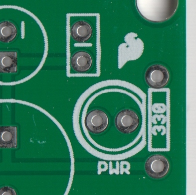
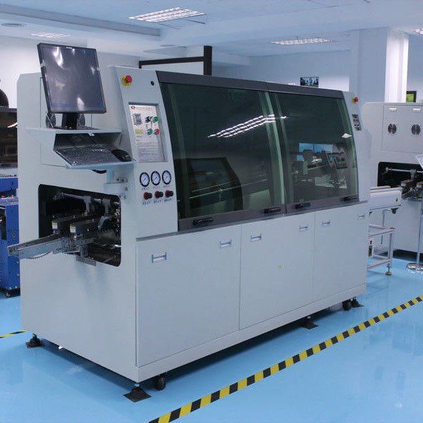
good quality wave welding solder alloy bar tin ingot
For soldering applications which require maximum reliability of solder joints, especially for surface mounted omponents, only solder of the highest purity is acceptable. We do not make any vague claims of outstanding solder purity. Complete analysis of Bar Solders prove that every batch conforms to the strictest quality control standards in the solder industry. Sn60Pb40 bar solder weight about 0.78kg/pc,package with 10kg per carton.
bar solders have been exported to such as Colombia,Mexico,Russia,Canada,Netherlands,Iran,Dubai,Saudi Arabia,Vietnam,if your are interested in our solders,pls send us e-mail through website,we will feedback to you within two working days.
Feature:
1. Favorable fatigue resistance and outstanding performance
2. Ultra high electrical conductivity
3. Mid-temperature soldering, characterized by nice softness and wonderful wetting property.
4. Benefit from activated rosin core flux.
5. Ultra strong oxygen resistance. Due to the anti-oxygen material in the solder wire,Sn63Pb37 no clean solder wire can give strong resistance to oxygen.
Low Dross Characteristics:giving cost effective use of the solder alloy.
Low Dross Characteristics:reducing the amount of dross in the wave pot leading to lower downturn and reducing the chance of oxide entrapped in joints.
Manufactured to Alpha’s high standards: giving a product that can be relied on to give good consistent soldering performance.
Chemical content:
Impurity content %
Sn
Pb
Sb
Ag
Cu
Fe
Zn
Bi
Al
As
Ni
Cd
60±2
40+/2
≤0.10%
≤0.02%
0.1%
≤0.02%
≤0.001%
≤0.10%
≤0.001%
≤0.03%
≤0.01%
<0.01%
59.3
bal
0.032
0.0002
0.0057
0.002
0.0015
0.006
0.0024
0.0021
0.0032
0.0001
Maximum Allowed Impurities
solder Bar Solder meets the requirements of current industry standards for allowable impurity requirements. Elements are considered impurities if they are not listed as components in the composition of the alloy.
Storage and Shelf Life:
Sn60Pb40 bar solder has no limited shelf life when handled properly.rage must be in a dry,non-corrosive environment. The solder surface may lose its shine and appear a dull shade of gray. This is a surface phenomenon and is not
detrimental to product functionality.
Tin-lead solder bar size as follow:
Alloy composition
Sn/Pb
Specific gravity
Liquid temperature
Temperature
Application
63/37
8.39
183
220~240
Computers, precision instruments, meters, TV,
60/40
8.65
190
230~250
micro technology, coating metals
55/45
8.75
200
240~260
Calculators, tape recorders, telephones, quartz and
50/50
8.85
216
255~275
other common electronic and electrical products
45/55
8.97
227
270~290
40/60
9.30
238
295~310
General circuit boards, toys, lamps, crafts, water tanks, plumbing solder
30/70
9.70
260
310~325
20/80
10.05
275
325~335
General circuit boards, toys, lamps, crafts, water tanks, plumbing solder
Solder product
Contact:
All emails will be answered within 24 hours.
Please leave a message in the Trade Manager.
If you do not receive our reply, please kindly re-sent your email and we will reply you as soon as possible . If you email us and dont hear a reply, please email again through the Alibaba system as sometimes our mail servers have errors
Tin-Bismuth-silver(Sn64Bi35Ag1) solder wire, with a melting point of 179 degrees C, is ideal for soldering of temperature sensitive components. Supplied as a solid core (no inner flux core) lead free solder wire, this solder gives good wetting and solder flow. Packaged as a 1000g box this solder wire we recommend using with the PF670 flux gel to promote increased rapid wetting.
Low temperature eutectic Tin Bismuth alloy Prevents thermal damage to heat sensitive devices Low to non-toxic lead free solder Available currently in a 0.5mm,0.6mm,0.8mm,1.2mm and 2.0mm diameter.
Packing:1kg/case
Feature of Sn64Bi35Ag1 no flux core Bismuth solder wire
The most popular lead-free bismuth solder alloys are BBI-W104 (58Bi 42Sn) which melts at 138°C and BBI-W105 (Sn64-Bi35Ag1) which melts at 179°C. The addition of the 1% Ag makes the alloy more malleable. Both alloys can be used for step soldering applications. After the initial joints are made with a standard SAC alloy (220°C) subsequent soldering operations can be done using the bismuth alloys.
Sn64Bi35Ag Bi solder wire has joint properties similar to those of tin-lead solders, with superior fatigue and copper dissolution characteristics.
Bismuth is the most diamagnetic and the least thermally conductive of all metals
In addition to being non-toxic it does not oxidize as readily as lead does.
Feature of other solder wire is also available for Low temperature eutectic Tin Bismuth silver alloy:
Excellent scalability
High quality soldering wire on the market
Refined welding good fluidity, wetting, smoke spatter
Excellent First Pass Solder Joints. JIS Spread ≥ 80%.
Quick acting flue dissolves surface oxides for good wetting
Good solderability, insulation resistance, No spattering and Non-corrosive.
Widely used in electrical and electronics, solder parts like circuit board, electronics devices and others.
More than 10 years specialized in metal industry, accumulated a lot of talent and technology, created international marketing network, for now, have cooperated with many of oversea enterprises of over 80 countries around the world.e.g.America,Israel,India,Germany,Russia,Poland,LTU,Switzerland,Korea,Romannia,Bulgaria,Colombia,France etc. Specification of Sn/Bi/Ag low temperature solder wire:
Item: Low temperature solder wire
Specification: BBI-W105(Sn64Bi35Ag1) 1. Purity and chemistry component
Specification
Sn64Bi35Ag1- no flux core solder wire
Appearance
Lucent,no dirt on surface
Weight
Net: 500g/case;1000g/case
Chemistry component
Elements Specification(%) Tested result(%WT)
Sn 63.0~65.0 64.0
Ag 0.8~1.2 1.0
Al 0.005 0.0003
As 0.030 0.0060
Sb 0.050 0.0148
Bi Remainder Remainder
Cu 0.080 0.0003
Fe 0.010 0.0003
In 0.050 0.0019
Ni 0.010 0.0007
Pb 0.050 0.0257
Cd 0.002 0.0002
Au 0.050 0.0010
Ag 0.050 0.0002
a. The above concentration of specification are in % weight.
b. Single value listed are the maximum allowable standard.Flux content(%): 0
Diameter of wire: 0.5mm,0.6mm,0.8mm,1.0mm,1.2mm and 2.0mm
Physical feature of Sn64Bi35Ag1 solid solder wire
Alloy component
Melting
point℃
Working temperature℃
Gravity g/cm3
Rigidity HB
Conduct heat
M.S.K
Extend
Mpa
Extend
rate
%
Conductivity %
Sn64Bi35Ag1
179
100~210
8.5~8.7
11~12
68
45
70-100
18.0
The more informations about Sn64Bi35Ag1 middle temperature metiong lead free solder wire,please feel freely contact with us.
Sn64Bi35Ag1 and other tin bismuth wire Application:
Advantages of Bismuth-based Alloys for Low Temperature Pb-free Soldering and Rework.
More and more requirment for middle and low temperature solder wire for moblie electronics,smart-home electronics..
The increased function of personal electronic devices, such as mobile phones and personal music devices, has driven the need for smaller and smaller active and passive components. This trend toward miniaturization, occurring at the same time as the conversion to RoHS-compliant lead-free assembly, has been a considerable challenge to the electronics assembly industry. The main reason for this is the higher reflow process temperatures required for Pb-free assembly. These higher temperatures can thermally damage the PCB and the components. In addition, the higher reflow temperatures can negatively affect the solder joint quality, especially when coupled with the smaller paste deposits required for these smaller components. If additional thermal processing is required, the risk increases even more.
Packing of tin-bismuth-silver solder wire
Product Type
Solder wire Sn64Bi35Ag
Material
Tin-Bismuth-Silver alloy
Composition
tin64%,bismuth 35%,silver 1%
Melt point
179degree
Flux content
no flux
Application
Metal soldering,electronics
Density (g/m^3)
8.3
Diameter
0.5mm,0.7mm,0.8mm,1.0mm,1.2mm,2.0mm
Packing
500g/case,1kg/case
Type
no flux core solder wire
Place of origin
Shenzhen,Dongguan city
Keyword
Tin bismuth silver lead free no flux core solder wire
To keep pace with rapid technological development in the electronic and electrical field Bhavani Metals manufactures Rosin Core solder Wire, ROHS Compliance Solder, Lead free solder, Solder Alloys, Silver Solder, Solder Paste and solder sticks with high grade pure virgin metals. Rigid analytical quality control procedure being exercised on every cast. Highly skilled technicians and engineers specialized in the field, properly check the quality and reliability of the rosin core solder wire, lead free solder & solder alloysto meet relevant standards.
Solder Wire can be supplied in Rosin activated / Urea based fluxes as per customer requirement in various Diameters upto 22 SWG with different combination of Tin / Lead / Silver / Cadimum / Antimony etc.
SRI BHAVANI Solder wires are manufactured in Solid, Single and Five Cores of Flux. The flux is uniformly distributed throughout the longitudinal axis of the Solder. The fluxes used are activated non corrosive and of fast spreading action.
Only high purity virgin metals are used in the manufacture.
Available in various metal combinations of Tin, Lead, Silver, Zinc etc.
SRI BHAVANI Solder Wire and Sticks are generally confirming to I. S. 1921 and I.S.193.
Solder Wires are available upto 22 SWG diameters. Solder Stick are of standard size.
Solder Sticks with Tin, Lead and Zinc combinations for Aluminium Soldering are available.
Solder Anodes and other alloys are also manufactured as per customer`s specifications.
Tin-silver-copper has received much publicity in recent years as the lead-free solder of choice. SAC305 was endorsed by the IPC Solder Value Product Council in the United States as the preferred option for SMT assembly; most assemblers have transitioned to this alloy for their solder paste requirements. The SAC305 alloy due to its 3.0% content of silver is expensive when compared to traditional 63/37 for this reason many wave assemblers are opting for less costly options such as tin-copper based solders for their wave, selective and dip tinning operations. In recent years tin-copper based solders with a variety of elemental additives have emerged which improve the overall properties and performance of tin-copper solders. Tin-copper solder without the incremental additions of certain elements is rarely used but the addition of nickel or nickel and bismuth as found for example in K100 and K100LD respectively do offer improvements in wetting, joint cosmetics and in some cases solder joint reliability. These alternative SnCu based solders are not normally used in reflow soldering but are gaining use globally in wave and selective soldering operations. This paper will describe how to achieve solder joint reliability using SnCu based solder with nickel and other additives such as bismuth.
Comparing
SAC and Tin-Copper Based Solders At this time there is no doubt more technical information exists for SAC solder. The number of users for SnCu based solders has steadily increased in recent years and about 30% of assemblers are now using various alternatives of SnCu solder in wave or selective systems. SAC solders still account for about 60% and 10% use other lead-free solders such as tin-silver and tinbismuth. However the rate of conversion to tin-copper has increased in 2006 and into 2007. What are the main differences between SAC and SnCu based solders? Is it as reliable as SAC in wave soldering applications? These are common questions often asked by engineers. One of the main attraction and difference is cost. Below is Figure 1 indicating the relative cost of SAC to SnCu. The cost of material will impact the initial cost of loading but also the operating costs of wave and selective systems. The approximate elemental concentrations of K100LD and K100 are detailed; it must be noted that very few use tin-copper solder without some additives.
The other difference is solder joint cosmetics. SAC solders tend to demonstrate various levels of solder shrinkage effects. Solder hot tears as documented in IPC-STD-610D are not considered a defect if the tear bottom can be seen during inspection or that the tear does not contact the board barrel or termination of the component. Examining the bottom of the tear is next to impossible to do since the tear is not always straight down and the other concern is the long term impact of thermal cycling on the hot tear. The photographs shown below Figure 2 and 3 indicate typical hot tears seen with SAC solder in wave soldering.
Solder PCB
Figure 3 shows solder joints using SAC305 after 500 thermal cycles; the fracturing seems to have aggravated but at this time it is not known if this will have an impact on long term joint reliability. These pictures are part of the iNemi Lead-free Wave Solder Project which is still ongoing. SnCu based solders with certain minute additives will show much lower levels of shrinkage. The shrinkage effect also happens when hand-soldering with SAC; SnCu based solders with additives does not do this. Other physical and chemical characteristics comparing SAC305 to two popular SnCu based solders are shown in Figure 4. Another advantage of these alloys is the lower reactivity to metals used in soldering equipment and also lower dissolution of copper. For example the dissolution rate for SAC305 is over 2 ½ times higher than SnCuNiBi. The lower dissolution rate of copper can increase the reliability of solder joints by preserving the metallization at the bond layers. In some cases such as fountain rework operations the dissolution of copper at the elbow of a through-hole barrel has at times been complete; resulting in a weaker bond. The erosion of copper happens more vigorously at the area of more solder flow, the elbow of the through-hole barrel.
The other advantages of lower dissolution rates for copper are reduced solder pot maintenance, less solder analysis frequency. The solder alloy remains more elementally uniform and a more consistent solder results in better process control. Less contamination of the solder is always a plus; copper dissolution also tends to increase the melting point of the lead-free solder. The higher melting point will result in a more sluggish flow of solder resulting in lesser hole-fill. The other difference is the wetting speed and SnCu based solders have slower wetting speeds than SAC solders. This does impact the process of solder in several ways and the optimization of contact time and immersion depth is more critical with SnCu. The optimization will be necessary to insure adequate hole-fill. If the soldering process is controlled carefully adequate hole-fill is possible with both SAC and SnCu based solders. However wetting speeds compared using a wetting balance tester show SAC having wetting speeds higher than SnCu based solders. This means that SAC alloys have a better chance of giving acceptable hole-fill in wave and selective systems. SnCu based solders will require at times different process parameters to achieve the same results as SAC solder. Below in Figure 5 are two wave soldered solder joints accomplished with SnCu based solder and SAC305. Both have complete hole-fill although SnCu based solder does have a slower wetting speed, the results are the same.
To summarize several other differences between both alloys Figure 6 shows the typical solder pot temperatures used to achieve the same results as with SAC solder. The longer contact time enables SnCu based solders to wet completely the through-hole part. The immersion depth of the board was also critical here and is best to use at least ½ of the board thickness. In thicker assemblies such as 0.093 inch or more ¾ is best. The flux used in soldering will also play an important role in hole-fill, the higher the activity and stability of the activators used in the flux formulation will enable better hole-fill. Since contact time is longer with SnCu based solders a flux designed for this application will perform better.
The impact of board finish and soldering will also be a factor with lead-free. Lead-free solders wet more slowly than leaded solders. Since SnCu based solders have slower wetting speeds than SAC, the choice of board finish, the number of heating cycles it sees and its storage and handling will impact its solderability. The higher the oxidation present on components and boards the mostly likely difficulties will be encountered with hole-fill and pad wetting using SnCu. The Figure7 shows the impact of soldering two finishes under similar conditions and it can be seen that copper OSP did not fair as well as the ENIG and AgImm board. We are a leader solder solution supplier in Shenzhen City China .
Assemblers Practical Experience with SnCu Based Solders At the assembler level once a product is required to be soldered with lead-free solders all the processes must be assessed as to insure the same level of quality as with Sn63Pb37. The reflow, wave soldering and hand assembly processes must all be optimized carefully to insure good joint formation as per the appropriate class of electronics with new solder alloys and new fluxes. Solder joint reliability must be assessed during the initial process validation. The validation of the wave solder process may include the following items. Alloy selection Flux selection Board and component finish selection and control Flux volume application Board and flux preheat requirements Solder temperature Use of chip wave or single wave Contact time at solder Immersion depth After wave soldering assemblers must verify the quality of the solder joints and these can be through-hole or bottom-side SMD’s. Each will have its own criteria of quality acceptance. Some basic tests which are normally performed are detailed below. Visual inspection X-ray analysis for voids Cross-sectional tests for bond verification Outside laboratory tests, IPC Class Inspection A successful build of 170,000 boards with SnCu based (Kester K100) was recently completed at a contract assembler. The board soldered with lead-free is described below. Board Type: 0.062 inch thick ENIG, ground plane on connector Board OEM: Printer board for FutureLogic Inc., a leading world wide manufacturer of thermal printers Components: Pure tin, matte tin, lead-free type SMD and through-hole parts The wave solder was lead-free capable and after loading with K100 lead-free solder it was analyzed to verify the elemental concentrations but also for the presence of iron or lead. The analysis revealed it was acceptable. Regular solder analysis is recommended with lead-free wave
soldering at least every 5000 board builds. A summary of the wave solder process is detailed below. Spray fluxing was used 5 sections of bottom-side convection heaters about 15 inches in width Quartz heater, before wave solder, width about 6 inches Chip wave, laminar wave Titanium solder pot and fingers No top preheaters 2 cooling blowers after wave solder pot 6° inclination used at the conveyor, adjustable No nitrogen blanketing was used To achieve good hole-fill and low defects the wave process needed to be carefully optimized. Lead-free solders wetting speeds are slower so traditional speeds used with Sn63Pb37 are not always suitable. Contact time and width are critical with lead-free alloys. The board impingement thickness is also important and this was revisited. Flux application was optimized to insure the spray applied flux uniformly and throughout the through-hole. An air-knife after the sprayer was not used but this can be useful if flux application is restricted in thicker boards or tighter hole-tolead ratios. With lead-free wave soldering flux application was found important. In this case alcohol based flux was used however VOC-free fluxes with higher surface tensions may benefit with the use on an air-knife. The parameters used in this build and which continued with the production of 170,000 boards are defined below.
Wave Solder Process Parameters: Conveyor Speed: 61 centimeters per minute. Solder temperature 265°C, only laminar wave used. Preheater settings WS-450PC-LF specific: 135, 140, 150, 155, 160 Top-side preheat board: 129-131°C. Solder contact width: 2 inches or 5.1 centimeters. Contact Time: 5 seconds Board thickness wave impingement: ½ to ¾ The hand-assembly of some connectors was accomplished after SMD and through-hole soldering using K100 water washable flux wire. The flux percentage is a critical element in wire solder selection and in this case the flux percentage was 3% by weight. Lower flux percentages make soldering with lead-free more difficult due to their slower wetting behaviors. Although tin-copper was used the wetting speed and solder joint quality were to IPC-610D Class 3 and 100% hole-fill was obtained throughout. Some of the basic criteria followed to obtain excellent lead-free hand-soldering are mentioned below. Lead-free compatible tips were used Correct tip geometry to achieve adequate thermal transfer Flux percent greater than 2% Soldering tip temperature 750ºF Marginally longer contact time No additional external flux was used Hand-soldering was used particularly to solder a connector which was lead-free finished and RoHS compliant but not lead-free process capable. To avoid plastic damage this part was handassembled and soldered.
An Electrovert AquaStorm 200 with DI water only, no chemical additives were used to clean-off all flux residues after soldering this included paste, liquid flux and wire flux residues. The water temperature used was 140°F. Cleanliness was measured using an ionic contamination tester and found to pass. In some cases residues tend to be more difficult to remove but in this case they removed well since the fluxes were lead-free process developed.
Figure shows the typical solder joints achieved with SnCu based solder using the previously indicated process parameters. The solder joints were free of shrinkage effects and were bright in finish. All solder joints met the IPC-STD-610D criteria for Class 3. Since the process was optimized carefully during the validation process, very few defects were encountered during the build of 170,000 assemblies. Thicker boards in the range of 0.093 inches and higher can be challenging with lead-free and another assembler successfully soldered a thicker board using SnCu based solder. The key to soldering thicker boards are the proper selection of flux, the setting up of the preheat temperature, contact time at the solder and board immersion depth. In some cases thicker boards will solder with better hole-fill with fluxes of higher activity or higher solids content. Another large contractor assembled a thicker board successfully with K100LD. This alloy is SnCu based with an addition of nickel and bismuth. The board for wave soldering is described as follows.
The board had also bottom-side SMD’s and these also exhibited excellent wetting without flagging, see Figure 12. Typical bridges and flagging can occur with lead-free solders if the flux is overheated during preheating or the activity of the flux is not sufficient to sustain the longer contact at the solder. Other issues encountered with thicker assemblies besides hole-fill, bridges and flagging are voids and solder mask blistering. The blistering is due to the slower conveyor speeds and longer contact times. Voids are generated for a variety of reasons but on thick boards the flow dynamics of a higher surface tension solder tend to create voids in the through-hole barrel. Tighter hole to lead ratios tend to give higher voids in thicker assemblies. A longer contact sometimes helps but not always. To summarize the main defects seen with thicker assemblies are:
Lack of hole-fill
Bridges and flagging
Voids
Mask blistering
Conclusions in the Use of SnCu Based Solders SnCu based solders particularly those containing certain additives can be a good choice in wave soldering applications. Solder joints can be created reliably is the whole process is optimized for the use with these solders. Although SnCu based materials have slower wetting than SAC type solders proper selection of board and component finishes including proper solderability management can enable the reliability of both through-hole and SMD parts. Hole-fill can be an issue with thicker boards but if the process is optimized with longer contact times and slower conveyor speeds. Here the flux selection is important since longer dwells at the wave solder tend to de-activate many fluxes. A flux designed for the soldering of thicker assemblies is recommended. Water washable and higher solids fluxes do tend to give better hole-fill. No-clean fluxes need to be chosen carefully and their performance at slightly higher solder temperatures used with SnCu based solders must be assessed in reference to hole-fill potential and other defects such as voids. SnCu based solders with additives to enhance soldering behavior can offer both bright joints free of shrinkage effects common with SAC solders and offer defect-free assemblies if the wave solder process is designed around them. In wave soldering SnCu based solders are an alternative to more costly SAC lead-free solders.
Usually thinner metal masks have a smaller amount of printed solder paste, resulting in lower thermal resistance and higher occurrence of unmolten solder. S3X05 is an easy-to-use solder paste where even a small amount melts well.
Effectively prevents “head-in-pillow” defects
S3X58-Sn 3.0Ag 0.5Cu easily coalesces with BGA balls even after left molten for 60 seconds. This proves the high thermal resistance of the solder paste where its activity is maintained for a long period of time even at high temperature, preventing “head-in-pillow” defects.this make your solder better than ever .
Improved stencil separation
The smaller solder powder size is,the bigger shear stress from the stencil surface becomes,thus making it vulnerable to printing failure In Sn 3.0Ag 0.5Cu solder paste ,lubricant additives in the flux attach to the aperture walls, and help solder paste separate from the stencil, enabling printing in high aspect ratio apertures. SAC305 will be much better than Original models .
Continuous printability of solder paste
We offer all kind of solder paste,Please contact us for better solution for you.
During the processing of our‘No-Clean Solder Wire’, strict quality control management and the advanced drawing process are implemented. Meanwhile, the ratio of both trace metals and impurity substances in the wires are precisely controlled and the welding flux in the wires is distributed uniformly to insure welding continuity. Besides a clean and tidy packing as well as a bright and smooth surface,Sn62Pb36Ag2 soft soldering wire, in welding process, also provide excellent wettability and weldability, keeping the process in a friendly environment of few smell, few smoke, few flitting, and non-toxic environment.
Diameter :0.5mm0.6mm0.8mm1.0mm.2.0mm
Tolerance0.020.020.030.030.04
Net Weight0.5kg、1.0kg
All kinds of wires(e.g. tin-lead, lead-free, flux core, solid core)
Feature of Sn62Pb36Ag2 lead silver solder wire:
Nontoxic and environment friendly、Low melting point and stabilitytidiness surface and not easy to tienon-flux pollutionno dross residual.
1.Applied in the field of low temperature electronics surface mounting technology, Such as tin- Lead hand soldering, PCB secondary soldering. Application to thermal cut-off、thermal protector、Capacitors heating fuse, etc.
2. – CHEMICAL CHARACTERISTICS :
2.1 Amount of Tin : 62%±0.6%
2.2 Amount of Lead : 36%±0.5%
2.3 Amount of Silver :2+/-0.5
2.3 Tin-lead-silver of first smelting purity
2.4 Chart of maximum impurities:
Sn
Ag
Pb
Pb
Bi
Fe
Zn
Al
As
Others
bal
2+/-0.5
36+/-1
0.10
0.10
0.02
0.001
0.2
0.03
0.05
2.4 Available types of incorporated flux:
Rosin Activated: RMA & RA
2.5 Amount of flux incorporated: BS441 Grades 1, 2 or 3
Sn62Pb36Ag2 middle melting soldering wire feature:
The middle-melting solder wire, provided with a lower melting point and easy to operate, is one of the mos energy saving solders for welding. It is commonly used in electronic components’ gradient welding as well as the welding of thebbienrmolabile parts such as LED, LCD, LNB, radiators, thermosensors, fire alarms, flexible plates, air-condition protectors and the parts for lightningproof and temperature control. In the solder wire, one of Compo’s unique technic known as the Metal Crystal Refinement Technology is adopted to toughen the Sn/Pb/Ag wire, eliminating its brittleness, thus providing the wire with a fine, clean and bright surface.
Electric Property
Volume resistance
Insulation resistance
Initial value
After treating*
Dielectric constant
Dielectric loss tangent
3.6×10¹⁶Ω·cm JIS K69111.2×1014Ω JIS Z3197
1.2×10¹²Ω
3.12/1MHZ JIS K6911
0.012/1MHZ JIS K6911
Preservation condition
10°C
To be strictly kept at less than
10°C in refrigerator
Epibond Surface Mount Adhesives in clude Dispensing and Frictioning /stencil using two kinds of techniques.
We make 30ml 200ml and 300ml per syringe packing.
RED GLUE ADHESIVE HAVE THE FOLLOWING FEATURE:
Very good stable curing shapes without stringing and slumping are achieved at super high speed dispensing and very small dots.
Stable adhesive strength can be obtained with a variety of SMD.
Long-term preservation stability is expected.
High heat-resistivity and excellent electric properties are possessed.
Usable for screen printing.
1) Much lower temperature curing is aimed at amd is practically possible.
2) Very good stable curing shapes without stringing and slumping are achieved at super high speed dispensing and very amall dots.
3) stable adhesive strength can be obtained with a variety of SMD.
4) Long-term preservation stability is expected.
5) High heat-resistivity and excellent electric properties are possessed.
SMT is a kind of single epoxy resin adhesive .
1)Usable for screen printing.
2)High heat-resistivity
3)high speed dispensin
polyesthylene SMT red glueis a kind of single epoxy resin adhesive .Good stable curing shapes without stringing, overflowing and slumping are achieved even at a super high speed and long time printing. Because of the “rarely cutting” bonding strength and very low humidity absorption, it is specially fit for SMT technology of porous printing in common temperature. Its shape can easily be controlled .We can not only expect a long-term preservation stability but also the excellent thermal resistance and electrical properties. Moreover it is good for environment protection for its safety, no solvent and no smelling.
CURE SPEED VS. TEMPERATURE
The following graph shows the rate of torque strength developed with time at different temperatures. These times are
defined from the moment the adhesive reaches cure temperature. In practice, total oven time may be longer to allow
for heat up period. GUIDELINES FOR HANDLING EPIBOND®SURFACE MOUNT ADHESIVES
REWORKING
Once cured, Epibond®adhesives can be removed from a printed circuit board by heating the board to approximately
80°C (176°F to 185oF). When the temperature of the surface mount component reaches 80°C (176°F), the adhesive
will be soft enough to permit component removal using a “lift and twist” method.
After removing the component, reapply heat to any remaining adhesive until it is soft. Residual material can then be
scraped off the board surfaceINK16′>
kinds of Epibond-Series Surface Mount Adhesives are designed for holding in place bottom side – and some mixed technology – surface mount components during the wave soldering process. Epibond are high-quality non-slumping and non-stringing surface mount technology adhesives applied by dot dispensing, printing equipment and pin transfer, giving consistent dot profile and fast curing.
CLEANING
Uncured adhesives can be easily removed from printed circuit boards, screens or stencils using Alpha SM-110,
isopropyl alcohol, acetone, NMP and a wide variety of other solvents and cleaning fluids. Huntsman Advanced
Materials is constantly working with manufacturers of solvents and cleaning fluids to test and identify new materials
that meet the needs of our customers. For an updated list of suggested cleaning materials, please contact the
Huntsman Product Information Hotline at 800-331-6810. Note:
○Shelf life:6Months.
○Store adhesive in a refrigerator keeping the temperature at 5±3℃
○This product may cause skin irritation to sensitive personnel.
○In case Seal-glo DTK-L978 gets in touch with skin,wash it thoroughly with soap and water.
○In case of eye contact,wash out with clean water and consult a medical doctor immediately.
Electronics Manufacturing Services (EMS). With a rich history as an EMS provider to the Defense, Aerospace, Medical and markets, API’s facilities are configured to successfully accommodate low/medium volume and high mix programs from large or small customers. API is dedicated to putting the customer first and has received many awards from our customers throughout the years.
Locations for API’s growing EMS manufacturing base include sites in New York, Pennsylvania and Mexico. Core competencies at these locations include SMT, TH, full systems integration, testing, and direct order fulfillment. Additionally, the Company provides NPI (New Product Introduction) services at each site, assisting our customers with product development efforts and design for manufacturing. API Technologies maintains industry certifications including ISO 9001:2008, AS9100 Rev C, IPC-A-610, J-STD-001, ANSI, ITAR registered and ISO 13485 (pending). Through an experienced labor force and high quality standards, API is able to provide complex manufacturing solutions for mission critcal customer requirements.
Build to Print
• CCA/PCBA & Electromechanical Assemblies
• Sub Assemblies & Final Product Assemblies
• Prototypes, Pilot Builds & Production Volumes
• Glass Microwave Integrated Circuits (GMIC)
• Low/High Temperature Co-Fired Ceramics
• Thick Film/Thin Film
• New Product Introduction (NPI) Support
• Turnkey &/or Consigned Material Management
One of the key concepts in electronics is the printed circuit board or PCB. It’s so fundamental that people often forget to explain what a PCB is. This tutorial will breakdown what makes up a PCB and some of the common terms used in the PCB world.
Over the next few pages, we’ll discuss the composition of a printed circuit board, cover some terminology, a look at methods of assembly, and discuss briefly the design process behind creating a new PCB.
Before you get started you may want to read up on some concepts we build upon in this tutorial:
What is Electricity?
What is a Circuit?
Voltage, Current, Resistance, and Ohm’s Law
Connector Basics
Soldering 101 – PTH
Signals
What’s a PCB?
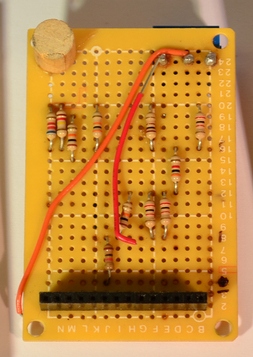
Printed circuit board is the most common name but may also be called “printed wiring boards” or “printed wiring cards”. Before the advent of the PCB circuits were constructed through a laborious process of point-to-point wiring. This led to frequent failures at wire junctions and short circuits when wire insulation began to age and crack.
A significant advance was the development of wire wrapping, where a small gauge wire is literally wrapped around a post at each connection point, creating a gas-tight connection which is highly durable and easily changeable.
As electronics moved from vacuum tubes and relays to silicon and integrated circuits, the size and cost of electronic components began to decrease. Electronics became more prevalent in consumer goods, and the pressure to reduce the size and manufacturing costs of electronic products drove manufacturers to look for better solutions. Thus was born the PCB.
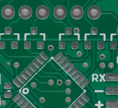
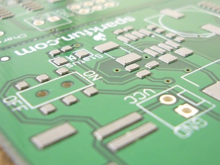
PCB is an acronym for printed circuit board. It is a board that has lines and pads that connect various points together. In the picture above, there are traces that electrically connect the various connectors and components to each other. A PCB allows signals and power to be routed between physical devices. Solder is the metal that makes the electrical connections between the surface of the PCB and the electronic components. Being metal, solder also serves as a strong mechanical adhesive.
Composition
A PCB is sort of like a layer cake or lasagna- there are alternating layers of different materials which are laminated together with heat and adhesive such that the result is a single object.
Let’s start in the middle and work our way out.
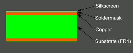
FR4
The base material, or substrate, is usually fiberglass. Historically, the most common designator for this fiberglass is “FR4”. This solid core gives the PCB its rigidity and thickness. There are also flexible PCBs built on flexible high-temperature plastic (Kapton or the equivalent).
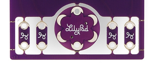
You will find many different thickness PCBs; the most common thickness for SparkFun products is 1.6mm (0.063″). Some of our products- LilyPad boards and Arudino Pro Micro boards- use a .8mm thick board.
Cheaper PCBs and perf boards (shown above) will be made with other materials such as epoxies or phenolics which lack the durability of FR4 but are much less expensive. You will know you are working with this type of PCB when you solder to it – they have a very distictive bad smell. These types of substrates are also typically found in low-end consumer electronics. Phenolics have a low thermal decomposition temperature which causes them to delaminate, smoke and char when the soldering iron is held too long on the board.
Copper
PCB with copper exposed, no solder mask or silkscreen.
The next layer is a thin copper foil, which is laminated to the board with heat and adhesive. On common, double sided PCBs, copper is applied to both sides of the substrate. In lower cost electronic gadgets the PCB may have copper on only one side. When we refer to a double sided or 2-layer board we are referring to the number of copper layers (2) in our lasagna. This can be as few as 1 layer or as many as 16 layers or more.
The copper thickness can vary and is specified by weight, in ounces per square foot. The vast majority of PCBs have 1 ounce of copper per square foot but some PCBs that handle very high power may use 2 or 3 ounce copper. Each ounce per square translates to about 35 micrometers or 1.4 thousandths of an inch of thickness of copper.
Soldermask
The layer on top of the copper foil is called the soldermask layer. This layer gives the PCB its green (or, at SparkFun, red) color. It is overlaid onto the copper layer to insulate the copper traces from accidental contact with other metal, solder, or conductive bits. This layer helps the user to solder to the correct places and prevent solder jumpers.
In the example above green solder mask is applied to the majority of the PCB, covering up the small traces but leaving the the silver rings and SMD pads exposed so they can be soldered to.
Soldermask is most commonly green in color but nearly any color is possible. We use red for almost all the SparkFun boards, white for the IOIO board, and purple for the LilyPad boards.
Silkscreen
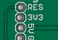
The white silkscreen layer is applied on top of the soldermask layer. The silkscreen adds letters, numbers, and symbols to the PCB that allow for easier assembly and indicators for humans to better understand the board. We often use silkscreen labels to indicate what the function of each pin or LED.
Silkscreen is most commonly white but any ink color can be used. Black, gray, red, and even yellow silkscreen colors are widely available; it is, however, uncommon to see more than one color on a single board.
Terminology
Now that you’ve got an idea of what a PCB structure is, let’s define some terms that you may hear when dealing with PCBs:
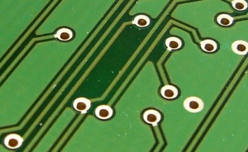
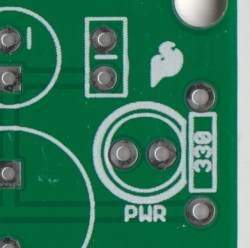
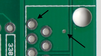
Annular ring – the ring of copper around a plated through hole in a PCB.
Examples of annular rings.
DRC – design rule check. A software check of your design to make sure the design does not contain errors such as traces that incorrectly touch, traces too skinny, or drill holes that are too small.
Drill hit – places on a design where a hole should be drilled, or where they actually were drilled on the board. Inaccurate drill hits caused by dull bits are a common manufacturing issue.
Not so accurate, but functional drill hits.
Finger – exposed metal pads along the edge of a board, used to create a connection between two circuit boards. Common examples are along the edges of computer expansion or memory boards and older cartridge-based video games.
Mouse bites – an alternative to v-score for separating boards from panels. A number of drill hits are clustered close together, creating a weak spot where the board can be broken easily after the fact. See the SparkFun Protosnap boards for a good example.
Mouse bites on the LilyPad ProtoSnap allow the PCB to be snapped apart easily.
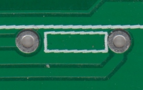
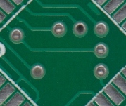
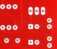
Pad – a portion of exposed metal on the surface of a board to which a component is soldered.
PTH (plated through-hole) pads on the left, SMD (surface mount device) pads on the right.
Panel – a larger circuit board composed of many smaller boards which will be broken apart before use. Automated circuit board handling equipment frequently has trouble with smaller boards, and by aggregating several boards together at once, they process can be sped up significantly.
Paste stencil – a thin, metal (or sometimes plastic) stencil which lies over the board, allowing solder paste to be deposited in specific areas during assembly.
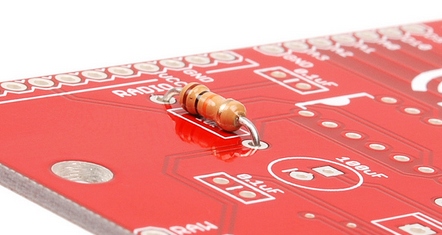
Plated through hole – a hole on a board which has an annular ring and which is plated all the way through the board. May be a connection point for a through hole component, a via to pass a signal through, or a mounting hole.
A PTH resistor inserted into the FabFM PCB, ready to be soldered. The legs of the resistor go through the holes. The plated holes can have traces connected to them on the front of the PCB and the rear of the PCB.
Pogo pin – spring-loaded contact used to make a temporary connection for test or programming purposes.
The popular pogo pin with pointed tip. We use tons of these on our test beds.
Reflow – melting the solder to create joints between pads and component leads.
Silkscreen – the letters, number, symbols and imagery on a circuit board. Usually only one color is available, and resolution is usually fairly low.
Silkscreen identifying this LED as the power LED.
Slot – any hole in a board which is not round. Slots may or may not be plated. Slots sometimes add to add cost to the board because they require extra cut-out time.
Complex slots cut into the ProtoSnap – Pro Mini. There are also many mouse bites shown. Note: the corners of the slots cannot be made completely square because they are cut with a circular routing bit.
Solder paste – small balls of solder suspended in a gel medium which, with the aid of a paste stencil, are applied to the surface mount pads on a PCB before the components are placed. During reflow, the solder in the paste melts, creating electrical and mechanical joints between the pads and the component.
Solder paste on a PCB shortly before the components are placed. Be sure to read about paste stencil above as well.
Solder pot – a pot used to quickly hand solder boards with through hole components. Usually contains a small amount of molten solder into which the board is quickly dipped, leaving solder joints on all exposed pads.
Soldermask – a layer of protective material laid over the metal to prevent short circuits, corrosion, and other problems. Frequently green, although other colors (SparkFun red, Arduino blue, or Apple black) are possible. Occasionally referred to as “resist”.
Solder mask covers up the signal traces but leaves the pads to solder to.
Solder jumper – a small, unwanted blob of solder connecting two adjacent pins on a component on a circuit board.
Surface mount – construction method which allows components to be simply set on a board, not requiring that leads pass through holes in the board. This is the dominant method of assembly in use today, and allows boards to be populated quickly and easily.
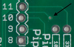
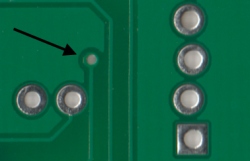
Thermal – a small trace used to connect a pad to a plane. If a pad is not thermally relieved, it becomes difficult to get the pad to a high enough temperature to create a good solder joint. An improperly thermally relieved pad will feel “sticky” when you attempt to solder to it, and will take an abnormally long time to reflow.
On the left, a solder pad with two small traces (thermals) connecting the pin to the ground plane. On the right, a via with no thermals connecting it completely to the ground plane.
Thieving – hatching, gridlines, or dots of copper left in areas of a board where no plane or traces exist. Reduces difficulty of etching because less time in the bath is required to remove unneeded copper.
Trace – a continuous path of copper on a circuit board.
A small trace connecting the Reset pad to elsewhere on the board. A larger, thicker trace connects to the 5V power pin.
V-score– a partial cut through a board, allowing the board to be easily snapped along a line.
Via – a hole in a board used to pass a signal from one layer to another. Tented vias are covered by soldermask to protect them from being soldered to. Vias where connectors and components are to be attached are often untented (uncovered) so that they can be easily soldered.
Front and back of the same PCB showing a tented via. This via brings the signal from the front side of the PCB, through the middle of the board, to the back side.
Wave solder – a method of soldering used on boards with through-hole components where the board is passed over a standing wave of molten solder, which adheres to exposed pads and component leads.
From a wide offer of solders from company Stannol , it´s easy to choose the most suitable type meeting your demands.
The solder matters, it is an undisputable fact confirmed daily in a development and production of electronics. Hand soldering of prototypes, automated machine soldering, soldering of small SMT components or on the in contrast soldering of big joints of massive connectors, rework, … all that wants a solder optimized for a given usage.
As we know, features of a solder wire are determined by an alloy itself (PbSn xx, SnAg xx, …) but in a considerable extent also a flux used. A flux has a big influence mainly on a soldering process, spreading of solder (often even on partially oxidized surfaces), spitting at hand soldering, etc. That´s why despite of often similar specification (according to datasheets), it is still possible to see considerable differences among solders after all. Besides the most important parameters like composition of alloy and flux properties, some features (like spitting and solder spreading) can be really evaluated only at working with a given type.
Over 130-years experience of German company Stannol give a guarantee, that in their portfolio can be found a type suitable even for your work. In a Stannol catalogue can be found favourite “universal” types suitable for the most types of works in electronics and electrotechnics (for example HS10, HF32, Kristall 400) but also specialized types suitable even for soldering of poorly solderable surfaces.
The principle of Stannol products marking is in it, that they are marked by a flux type (HS10, HF32,…) and by an alloy used (Snxx, SnPb,…). A solder wire is available in many combinations flux / alloy , that´s why it is suitable look at their properties in detail and then to choose a suitable type. On stock we keep the most favorite types with fluxes HS10, HF32 or 2630, suitable for ,majority of joints.