The information on the page was last updated 16 March 2020.
Basic hygiene measures are the most important way to stop the spread of infections, including the 2019 novel coronavirus (COVID-19). Basic hygiene measures include:
hand hygiene – that is, washing hands regularly with soap and water, or cleansing with hand sanitiser
staying at home if you are sick
coughing or sneezing into a tissue or your elbow and then performing hand hygiene
cleaning surfaces regularly.
The use of personal protective equipment (PPE), such as face masks can reduce the spread of infection when used correctly and in the appropriate context. This may be recommended in workplaces where people are more likely to come in contact with the disease.
Use of face masks
For most people in the community, PPE such as face masks are not recommended. However, for people with symptoms of an acute respiratory infection, the WHO recommends that there may be benefict in wearing a face mask to reduce the spread of infection to other people.
How to correctly wear and remove a face mask
If you are unwell or have a job which requires you to be in close contact with people who may have coronavirus, it is recommended you use a face mask. It is important that face masks are worn and removed correctly. Masks should fit snugly and fully cover your nose and mouth.
How to wear a mask:
wash hands with soap and water or use hand sanitiser
place over nose, mouth and chin
fit flexible nose piece over nose bridge
secure on head with ties or elastic
adjust to fit – secure on your head, fitting snugly around your face with no gaps
avoid touching or adjusting your mask during use.
How to remove a mask:
wash hands with soap and water or use hand sanitiser
avoid touching the front of the mask
if the mask has ties, untie the bottom, then top tie
remove from face
discard, do not use again
wash hands with soap and water or use hand sanitiser immediately.
Use of PPE in the workplace
Workplaces where people can maintain more than 2 metres contact distance from people with potential COVID19 symptoms – Facemasks and gloves are not recommended.
Examples of these workplaces include – education facilities, pharmacies, retail outlets
People who, due to the nature of their job, may be unable to maintain more than 2 metres contact distance from people with potential COVID19 symptoms – facemasks and gloves are recommended when this contact is likely to occur.
Examples of these workplaces include – Police, prison staff, customs staff
These recommendations are a guide only and workplace settings not listed in the table should consider their ability to maintain the 2 metres rule and use the table to inform their use of PPE. In general, surgical/medical masks prevent the dispersal of droplets by an infected patient and the inhalation of droplets if within 2 metres of a coughing individual.
Hand hygiene and cough / sneeze etiquette (maintain distance, cover coughs and sneezes with disposable tissues and wash hands) will have a bigger impact.
We hope all of us can be well from this case. If you need any more products information,pls feel free contact us.
Because it seems to be so many types of solder out there, choosing which solder to purchase can be confusing.
When I started out in electronics I had no clue, so I just used whatever solder I could find. But did you know that solder is not only used for soldering electronics?
Actually, solder is also used for plumbing.
And the solder used for plumbing should definitely not be used for electronics as it contains acid!
The main solder types
There are just a few basic points you need to know to understand what solder to choose and what to stay away from.
First of all, solder comes in many forms: pellets, bars, paste and wire. As a hobbyist, you will only need to get acquainted with the solder wire. And maybe the solder paste if you want to do SMD soldering.
There are two main types of solder:
Lead-based solder
Lead-free solder
The main practical difference between the two is the melting temperature. So in essence, you can choose whichever you like.
Lead-based solder
Solder based on lead was universally used in the past. It was made of a mixture of tin and lead. Usually a 60/40 (tin/lead) mix, that melts at around 180-190C degrees.
Because lead has some damaging effects to our health, the industry is moving away from lead and towards lead-free solder.
Lead-free solder
Lead-free solder is solder without lead. EU requires commercially available electronics to use lead-free solder (RHoS) because of the health hazards of lead.
It has a higher melting point, so it is a bit harder to work with, but usually not a problem.
The flux core of solder wires
Solder wires usually have a core inside the wire containing flux. Flux is designed to improve electrical contact and mechanical strength in solder joints.
There are mainly two types of flux cores. Acid core and rosin core. Acid core is used for plumbing and rosin core is used for electronics. So use rosin core.
(Side note: A new water-soluble flux core is starting to gain some traction as an alternative to rosin core because it is more environmental friendly.)
Summary
The main types of solder are lead and lead-free. You can use both for electronics, but it can be easier to work with lead-based solder.
Make sure to stay away from acid core solder as this is intended for plumbing, NOT electronics.
Here is a couple of alternatives I have found that should work very well for basic soldering:
NOF and solder mounting materials
Many alloys are under consideration as replacements for lead-based solder.working on tin-alloys, which have a melting point near that of lead-based solder and provide the opportunity to use NOF’s expertise in blocked carboxylic acid technology. Research is focusing on ways to solve the problem of metal deterioration caused by a chemical reaction with the carboxylic acid contained in the flux.
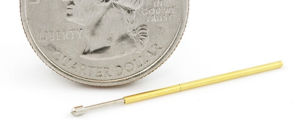
Solder particle
What is solder?
Solder is an age-old technique used to connect two types of metals. In the electronics industry, solder is used to attach electronic components to copper circuit lines on printed circuit boards.
What is solder
All about flux
Flux is a compound that includes carboxylic acid, often from rosin made from pine sap. Flux performs the following functions that are essential to linking two surfaces using solder.
Rosin
Using rosin or other chemical compounds containing carboxylic acid, flux plays a vital role in soldering as shown below.
Surface tension of solder coated by molten flux
Functions of flux
(1) Removes the oxide film from metal surfaces 2RCOOH + Cu2O -> 2RCOOCu + H2O
(2) Prevents oxidation by coating the solder
(3) Lowers surface tension
What is solder paste?
Solder paste is made by mixing a fine solder powder with liquid flux to produce a compound with a paste-like consistency. This paste is printed on the copper circuit pattern where components are to be mounted. Once components are in place, the board is heated to melt the metal in the solder and hold the components to the board.
Improvements in solder composition
An alloy of tin and lead was commonly used for many years but is no longer acceptable due to environmental issues. Companies are being required to switch to solder alloys that do not incorporate lead.
Harmfull things
Due to problems associated with reliability of the metal following
attachment, and to other issues, interest is currently focused on tin-silver compounds that have a melting point about 40°C to 50°C higher than lead-based solder. As a result, improvements are needed to make components that are resistant to higher temperatures and to enhance the performance of soldering ovens.
In addition, some companies have started studying tin-zinc compounds because they can be used with existing soldering ovens.
Indium Indium8.9HF is a halogen-free, no-clean solder paste that is specifically formulated to Avoid the Void™, while delivering high transfer efficiency with low variability.
In addition to outstanding print transfer and response-to-pause, this no-clean solder paste also provides excellent pin-in-paste solderability and hole-fill, while remaining stable at room temperature for up to 30 days.
Indium8.9HF is perfectly suited for a variety of applications, especially automotive, due to its unique oxidation barrier technology. This solder paste delivers robust reflow capability and a wide process window, accommodating various board sizes and throughput requirements, minimizing potential defects.
Indium8.9HF solder paste is part of our family of high-performance, lead-free, low-voiding, no-clean solder pastes that help manufacturers to Avoid the Void. For more information about Indium8.9HF, email us or visit solder1.wordpress.com.
We are a premier materials manufacturer and supplier to the global electronics, semiconductor, thin-film, thermal management, and solar markets. Products include solders and fluxes; brazes; thermal interface materials; sputtering targets; indium, gallium, germanium, and tin metals and inorganic compounds; and NanoFoil. Founded in 1934, Indium has global technical support and factories located in China,India Malaysia, Singapore,Japan,Germany, the United Kingdom, and the USA.
Electronics Manufacturing Services (EMS). With a rich history as an EMS provider to the Defense, Aerospace, Medical and markets, API’s facilities are configured to successfully accommodate low/medium volume and high mix programs from large or small customers. API is dedicated to putting the customer first and has received many awards from our customers throughout the years.
Locations for API’s growing EMS manufacturing base include sites in New York, Pennsylvania and Mexico. Core competencies at these locations include SMT, TH, full systems integration, testing, and direct order fulfillment. Additionally, the Company provides NPI (New Product Introduction) services at each site, assisting our customers with product development efforts and design for manufacturing. API Technologies maintains industry certifications including ISO 9001:2008, AS9100 Rev C, IPC-A-610, J-STD-001, ANSI, ITAR registered and ISO 13485 (pending). Through an experienced labor force and high quality standards, API is able to provide complex manufacturing solutions for mission critcal customer requirements.
Build to Print
• CCA/PCBA & Electromechanical Assemblies
• Sub Assemblies & Final Product Assemblies
• Prototypes, Pilot Builds & Production Volumes
• Glass Microwave Integrated Circuits (GMIC)
• Low/High Temperature Co-Fired Ceramics
• Thick Film/Thin Film
• New Product Introduction (NPI) Support
• Turnkey &/or Consigned Material Management
One of the key concepts in electronics is the printed circuit board or PCB. It’s so fundamental that people often forget to explain what a PCB is. This tutorial will breakdown what makes up a PCB and some of the common terms used in the PCB world.
Over the next few pages, we’ll discuss the composition of a printed circuit board, cover some terminology, a look at methods of assembly, and discuss briefly the design process behind creating a new PCB.
Before you get started you may want to read up on some concepts we build upon in this tutorial:
What is Electricity?
What is a Circuit?
Voltage, Current, Resistance, and Ohm’s Law
Connector Basics
Soldering 101 – PTH
Signals
What’s a PCB?
Printed circuit board is the most common name but may also be called “printed wiring boards” or “printed wiring cards”. Before the advent of the PCB circuits were constructed through a laborious process of point-to-point wiring. This led to frequent failures at wire junctions and short circuits when wire insulation began to age and crack.
A significant advance was the development of wire wrapping, where a small gauge wire is literally wrapped around a post at each connection point, creating a gas-tight connection which is highly durable and easily changeable.
As electronics moved from vacuum tubes and relays to silicon and integrated circuits, the size and cost of electronic components began to decrease. Electronics became more prevalent in consumer goods, and the pressure to reduce the size and manufacturing costs of electronic products drove manufacturers to look for better solutions. Thus was born the PCB.
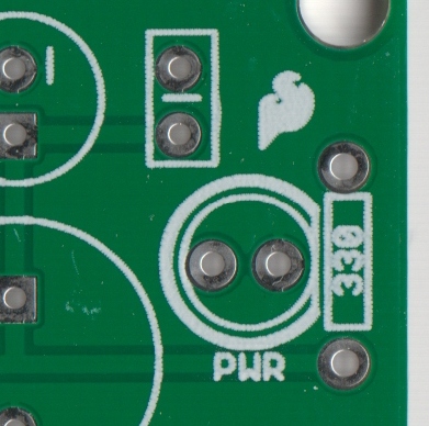
PCB is an acronym for printed circuit board. It is a board that has lines and pads that connect various points together. In the picture above, there are traces that electrically connect the various connectors and components to each other. A PCB allows signals and power to be routed between physical devices. Solder is the metal that makes the electrical connections between the surface of the PCB and the electronic components. Being metal, solder also serves as a strong mechanical adhesive.
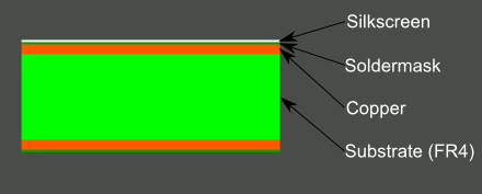
Composition
A PCB is sort of like a layer cake or lasagna- there are alternating layers of different materials which are laminated together with heat and adhesive such that the result is a single object.
Let’s start in the middle and work our way out.
FR4
The base material, or substrate, is usually fiberglass. Historically, the most common designator for this fiberglass is “FR4”. This solid core gives the PCB its rigidity and thickness. There are also flexible PCBs built on flexible high-temperature plastic (Kapton or the equivalent).
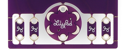
You will find many different thickness PCBs; the most common thickness for SparkFun products is 1.6mm (0.063″). Some of our products- LilyPad boards and Arudino Pro Micro boards- use a .8mm thick board.
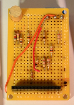
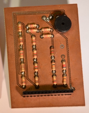
Cheaper PCBs and perf boards (shown above) will be made with other materials such as epoxies or phenolics which lack the durability of FR4 but are much less expensive. You will know you are working with this type of PCB when you solder to it – they have a very distictive bad smell. These types of substrates are also typically found in low-end consumer electronics. Phenolics have a low thermal decomposition temperature which causes them to delaminate, smoke and char when the soldering iron is held too long on the board.
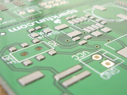
Copper
PCB with copper exposed, no solder mask or silkscreen.
The next layer is a thin copper foil, which is laminated to the board with heat and adhesive. On common, double sided PCBs, copper is applied to both sides of the substrate. In lower cost electronic gadgets the PCB may have copper on only one side. When we refer to a double sided or 2-layer board we are referring to the number of copper layers (2) in our lasagna. This can be as few as 1 layer or as many as 16 layers or more.
The copper thickness can vary and is specified by weight, in ounces per square foot. The vast majority of PCBs have 1 ounce of copper per square foot but some PCBs that handle very high power may use 2 or 3 ounce copper. Each ounce per square translates to about 35 micrometers or 1.4 thousandths of an inch of thickness of copper.
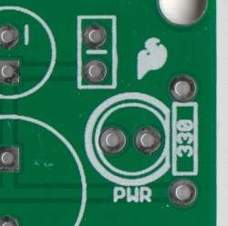
Soldermask
The layer on top of the copper foil is called the soldermask layer. This layer gives the PCB its green (or, at SparkFun, red) color. It is overlaid onto the copper layer to insulate the copper traces from accidental contact with other metal, solder, or conductive bits. This layer helps the user to solder to the correct places and prevent solder jumpers.
In the example above green solder mask is applied to the majority of the PCB, covering up the small traces but leaving the the silver rings and SMD pads exposed so they can be soldered to.
Soldermask is most commonly green in color but nearly any color is possible. We use red for almost all the SparkFun boards, white for the IOIO board, and purple for the LilyPad boards.
Silkscreen
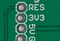
The white silkscreen layer is applied on top of the soldermask layer. The silkscreen adds letters, numbers, and symbols to the PCB that allow for easier assembly and indicators for humans to better understand the board. We often use silkscreen labels to indicate what the function of each pin or LED.
Silkscreen is most commonly white but any ink color can be used. Black, gray, red, and even yellow silkscreen colors are widely available; it is, however, uncommon to see more than one color on a single board.
Terminology
Now that you’ve got an idea of what a PCB structure is, let’s define some terms that you may hear when dealing with PCBs:
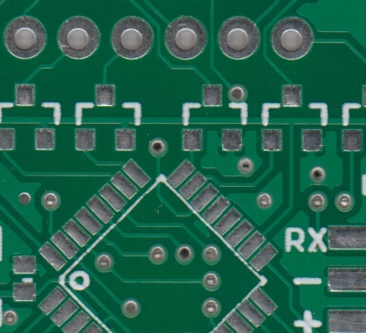
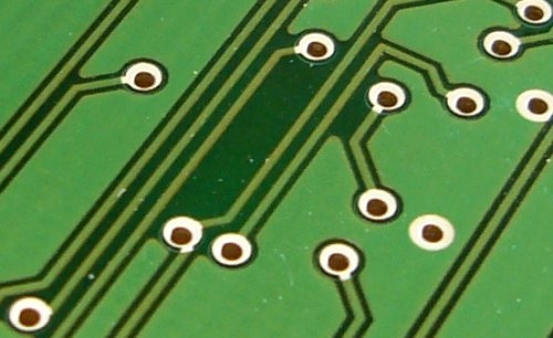
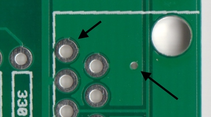
Annular ring – the ring of copper around a plated through hole in a PCB.
Examples of annular rings.
DRC – design rule check. A software check of your design to make sure the design does not contain errors such as traces that incorrectly touch, traces too skinny, or drill holes that are too small.
Drill hit – places on a design where a hole should be drilled, or where they actually were drilled on the board. Inaccurate drill hits caused by dull bits are a common manufacturing issue.
Not so accurate, but functional drill hits.
Finger – exposed metal pads along the edge of a board, used to create a connection between two circuit boards. Common examples are along the edges of computer expansion or memory boards and older cartridge-based video games.
Mouse bites – an alternative to v-score for separating boards from panels. A number of drill hits are clustered close together, creating a weak spot where the board can be broken easily after the fact. See the SparkFun Protosnap boards for a good example.
Mouse bites on the LilyPad ProtoSnap allow the PCB to be snapped apart easily.
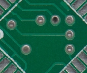
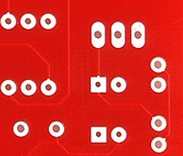
Pad – a portion of exposed metal on the surface of a board to which a component is soldered.
PTH (plated through-hole) pads on the left, SMD (surface mount device) pads on the right.
Panel – a larger circuit board composed of many smaller boards which will be broken apart before use. Automated circuit board handling equipment frequently has trouble with smaller boards, and by aggregating several boards together at once, they process can be sped up significantly.
Paste stencil – a thin, metal (or sometimes plastic) stencil which lies over the board, allowing solder paste to be deposited in specific areas during assembly.
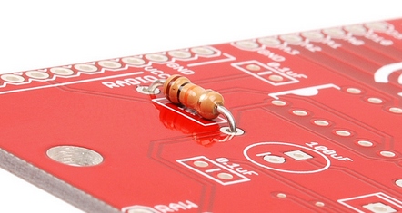
Plated through hole – a hole on a board which has an annular ring and which is plated all the way through the board. May be a connection point for a through hole component, a via to pass a signal through, or a mounting hole.
A PTH resistor inserted into the FabFM PCB, ready to be soldered. The legs of the resistor go through the holes. The plated holes can have traces connected to them on the front of the PCB and the rear of the PCB.
Pogo pin – spring-loaded contact used to make a temporary connection for test or programming purposes.
The popular pogo pin with pointed tip. We use tons of these on our test beds.
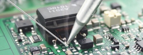
Reflow – melting the solder to create joints between pads and component leads.
Silkscreen – the letters, number, symbols and imagery on a circuit board. Usually only one color is available, and resolution is usually fairly low.
Silkscreen identifying this LED as the power LED.
Slot – any hole in a board which is not round. Slots may or may not be plated. Slots sometimes add to add cost to the board because they require extra cut-out time.
Complex slots cut into the ProtoSnap – Pro Mini. There are also many mouse bites shown. Note: the corners of the slots cannot be made completely square because they are cut with a circular routing bit.
Solder paste – small balls of solder suspended in a gel medium which, with the aid of a paste stencil, are applied to the surface mount pads on a PCB before the components are placed. During reflow, the solder in the paste melts, creating electrical and mechanical joints between the pads and the component.
Solder paste on a PCB shortly before the components are placed. Be sure to read about paste stencil above as well.
Solder pot – a pot used to quickly hand solder boards with through hole components. Usually contains a small amount of molten solder into which the board is quickly dipped, leaving solder joints on all exposed pads.
Soldermask – a layer of protective material laid over the metal to prevent short circuits, corrosion, and other problems. Frequently green, although other colors (SparkFun red, Arduino blue, or Apple black) are possible. Occasionally referred to as “resist”.
Solder mask covers up the signal traces but leaves the pads to solder to.
Solder jumper – a small, unwanted blob of solder connecting two adjacent pins on a component on a circuit board.
Surface mount – construction method which allows components to be simply set on a board, not requiring that leads pass through holes in the board. This is the dominant method of assembly in use today, and allows boards to be populated quickly and easily.
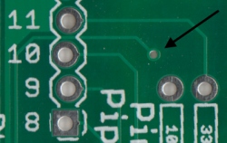
Thermal – a small trace used to connect a pad to a plane. If a pad is not thermally relieved, it becomes difficult to get the pad to a high enough temperature to create a good solder joint. An improperly thermally relieved pad will feel “sticky” when you attempt to solder to it, and will take an abnormally long time to reflow.
On the left, a solder pad with two small traces (thermals) connecting the pin to the ground plane. On the right, a via with no thermals connecting it completely to the ground plane.
Thieving – hatching, gridlines, or dots of copper left in areas of a board where no plane or traces exist. Reduces difficulty of etching because less time in the bath is required to remove unneeded copper.
Trace – a continuous path of copper on a circuit board.
A small trace connecting the Reset pad to elsewhere on the board. A larger, thicker trace connects to the 5V power pin.
V-score– a partial cut through a board, allowing the board to be easily snapped along a line.
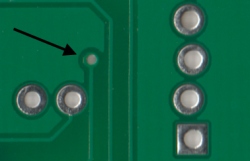
Via – a hole in a board used to pass a signal from one layer to another. Tented vias are covered by soldermask to protect them from being soldered to. Vias where connectors and components are to be attached are often untented (uncovered) so that they can be easily soldered.
Front and back of the same PCB showing a tented via. This via brings the signal from the front side of the PCB, through the middle of the board, to the back side.
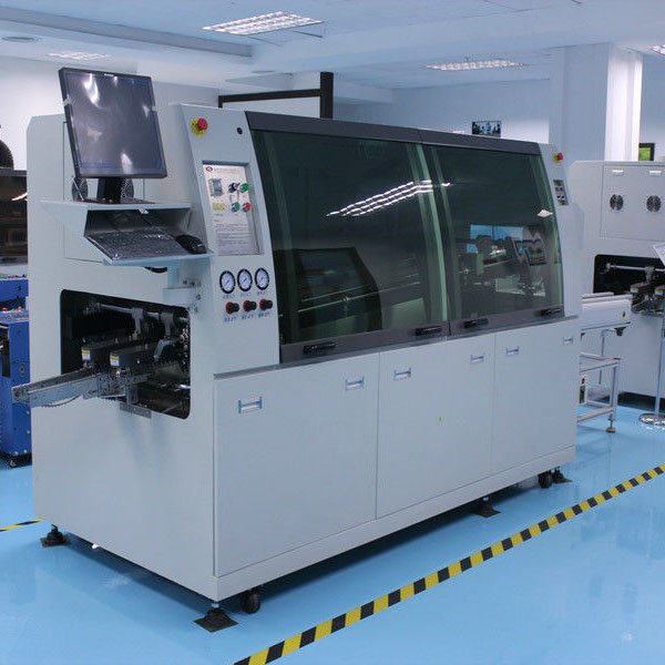
Wave solder – a method of soldering used on boards with through-hole components where the board is passed over a standing wave of molten solder, which adheres to exposed pads and component leads.
From a wide offer of solders from company Stannol , it´s easy to choose the most suitable type meeting your demands.
The solder matters, it is an undisputable fact confirmed daily in a development and production of electronics. Hand soldering of prototypes, automated machine soldering, soldering of small SMT components or on the in contrast soldering of big joints of massive connectors, rework, … all that wants a solder optimized for a given usage.
As we know, features of a solder wire are determined by an alloy itself (PbSn xx, SnAg xx, …) but in a considerable extent also a flux used. A flux has a big influence mainly on a soldering process, spreading of solder (often even on partially oxidized surfaces), spitting at hand soldering, etc. That´s why despite of often similar specification (according to datasheets), it is still possible to see considerable differences among solders after all. Besides the most important parameters like composition of alloy and flux properties, some features (like spitting and solder spreading) can be really evaluated only at working with a given type.
Over 130-years experience of German company Stannol give a guarantee, that in their portfolio can be found a type suitable even for your work. In a Stannol catalogue can be found favourite “universal” types suitable for the most types of works in electronics and electrotechnics (for example HS10, HF32, Kristall 400) but also specialized types suitable even for soldering of poorly solderable surfaces.
The principle of Stannol products marking is in it, that they are marked by a flux type (HS10, HF32,…) and by an alloy used (Snxx, SnPb,…). A solder wire is available in many combinations flux / alloy , that´s why it is suitable look at their properties in detail and then to choose a suitable type. On stock we keep the most favorite types with fluxes HS10, HF32 or 2630, suitable for ,majority of joints.